
- HOME
-
Company
Corporate Information - Life Science
- Electronic Materials
-
IR
-
Sustainability


×
Company
Corporate Information
IR
Sustainability
Our philosophy of "Curiosity, For a Bright Future” drives everything we do.
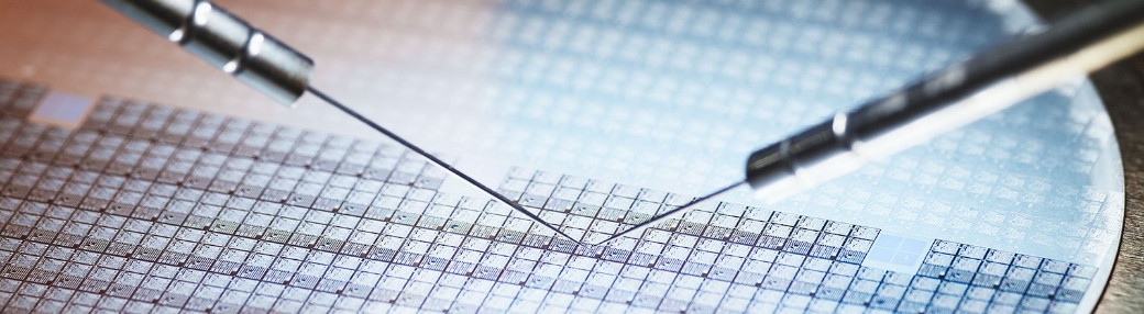
Building on decades of expertise, we have developed our flagship product, ”Quartron® Ultra High Purity Colloidal Silica” that has become indispensable in the semiconductor industry.
Since 1987, we have been dedicated to the research and development of “Quartron® Ultra High Purity Colloidal Silica”, which has secured a leading market share as the abrasive in final polishing slurry for silicon wafers. This cutting-edge technology plays an important role in the semiconductor manufacturing process, particularly in CMP (Chemical Mechanical Planarization), a polishing process demanding nanometer-level surface precision. Quartron® has been contributed to the multilayering and high integration of key components such as memory and CPU.
Through the development and production of advanced materials such as “Quartron® Ultra High Purity Colloidal Silica”, we have cultivated proprietary technologies and expertise that we now apply across various industrial applications. This has allowed us to establish a unique position in the field of functional chemical products.
Our advanced proprietary technologies, including specialized reaction methods, powder processing techniques, particle surface property control, purification technologies, and environmental solutions, enable us to manufacture precision chemical products. These technologies support a wide range of applications in industries such as electronics, cosmetics, pharmaceuticals, and plastics.
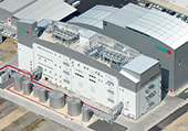
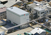
Developing and producing these product lines require highly precise analytical techniques, along with advanced production technologies, safety management systems, and environmental protection measures. At FUSO, we harness the expertise of our highly skilled engineers and optimize the operation of production facilities. Through this commitment, we deliver high-quality products that meet the diverse needs of society.